One-port acoustic resonators
Imaging acoustic leakage and higher-order modes in gigahertz resonators, and designing and fabricating an AlN-on-silicon resonator.
TMIM · Device design · Fabrication
This project has two parts that involve different devices. First, I imaged an existing X-cut LiNbO₃-on-SiC resonator, in collaboration with Prof. Ruochen Lu. Second, I designed and fabricated my own AlN-on-silicon resonator.
Imaging leakage in a gigahertz resonator

A resonator’s performance is limited by the energy that escapes it. An electrical spectrum (Y₁₁) shows that there are losses and spurious modes, but not where the energy goes.
Using TMIM on a one-port X-cut LiNbO₃-on-SiC resonator, I imaged the acoustic field both inside the resonator and just outside its reflectors. I did this at frequencies around the main resonance (about 1.03 GHz) and around the higher-frequency features (about 1.13 GHz) in the spectrum. This gives a direct, real-space picture of leakage.
The inside and outside maps use different color scales (±1 V and ±0.1 V), so their contrast should not be read as a calibrated leakage ratio.

Before interpreting weak signals outside the device, I characterized the noise floor of the measurement by sweeping the input power down to about −87 dBm.
Higher-order modes inside the resonator

Inside the resonator cavity, the TMIM maps show field variation across the aperture, not only along the propagation direction. This is the fingerprint of transverse higher-order modes, a common source of spurious responses in SAW resonators. Comparing the measured CH1/CH2 patterns with the simulated mode shape identifies which mode is excited.
Designing an AlN-on-silicon resonator

I then designed my own one-port resonator on a 200 nm AlN film on silicon. Using COMSOL, I simulated the dispersion of the guided acoustic mode to choose the IDT period. A wavelength of 3.6 µm places the resonance near 1 GHz in the simulated admittance spectrum. From the simulation I drew the CAD mask: a central IDT flanked by reflector gratings.
Fabrication

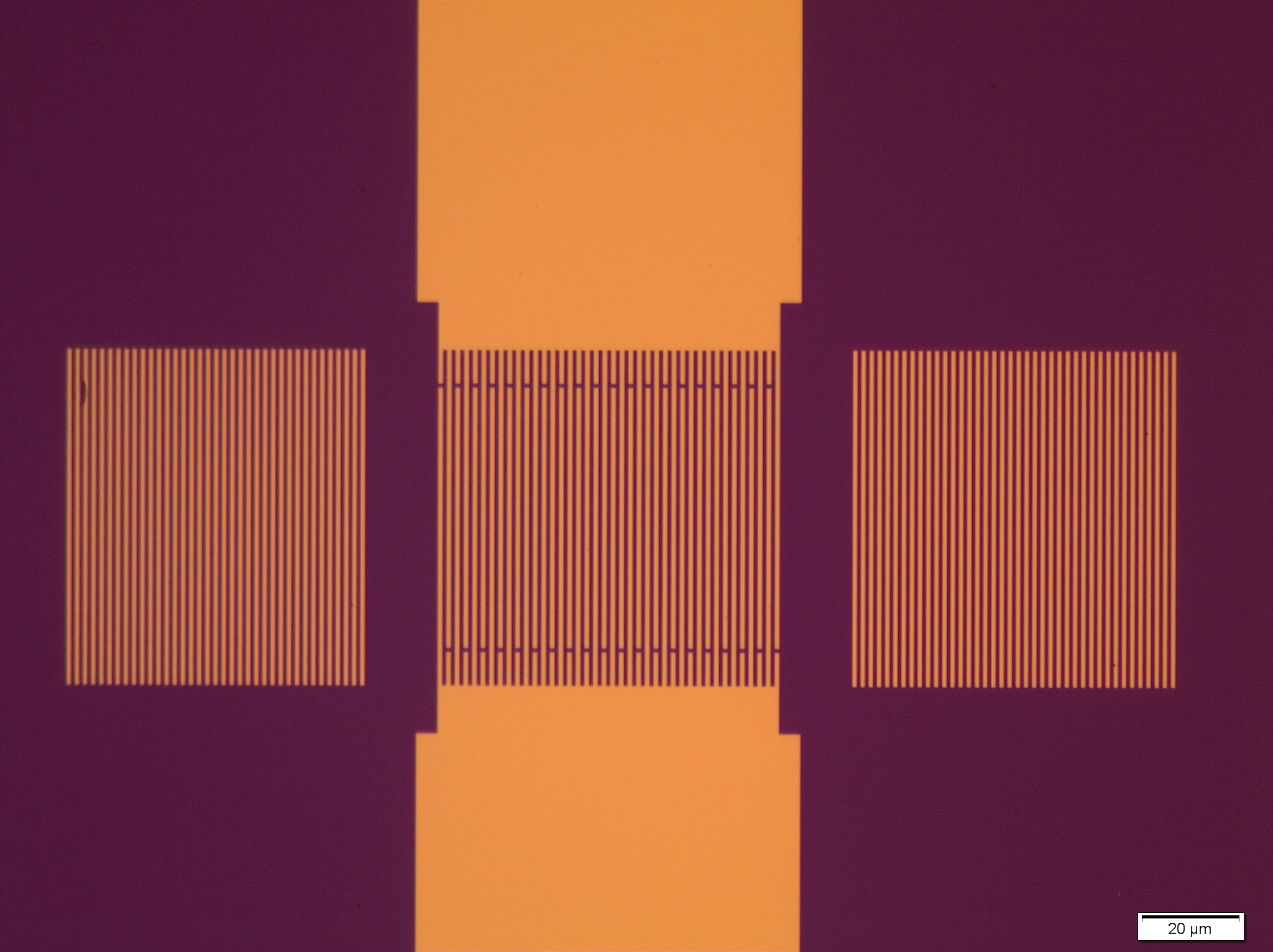
I fabricated the device using:
- Electron-beam lithography on PMMA resist.
- Deposition of 10 nm Cr / 100 nm Au, followed by lift-off.
The optical image shows the finished resonator: a central IDT, flanking reflectors, and contact pads.
Project status — August 2024
Leakage and higher-order modes were imaged in the LiNbO₃ resonator, and the AlN-on-silicon resonator was designed and fabricated. Next steps were electrical characterization of the AlN device, remeasuring the sample, and preparing a standard sample for low-temperature measurements.