Inverse-designed acoustic splitters
Designing acoustic scattering patterns and translating simulated geometries into multilayer fabrication masks.
Inverse design · MATLAB–COMSOL
Inverse design in photonics

In conventional design, a designer picks a structure and simulates what it does. Inverse design reverses the process: you specify what the device should do, and an algorithm searches for a structure that does it. In integrated photonics, this approach has produced ultra-compact wavelength and mode demultiplexers with irregular, non-intuitive patterns that a person would be unlikely to draw.
An inverse-designed acoustic power splitter

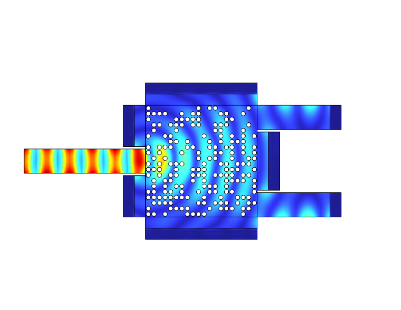
I asked whether the same idea works for gigahertz acoustic waves: can a patterned scattering region split acoustic power between two outputs in a chosen ratio? The design region is a 20 × 20 grid of scattering units in a 200 nm AlN film. Each unit is either a hole or no hole, and the hole diameter d and cell size a are additional parameters. An input waveguide feeds the region, and two output waveguides collect the power.
I built the design workflow in MATLAB and COMSOL: MATLAB coordinates the design loop, and COMSOL models the acoustic response of each candidate geometry.

In a first round, I simulated candidate patterns with an A0-mode input at 1 GHz and 10 mW, with PMLs absorbing the power at each output. I measured the power reaching each output against a target split ratio of 9 : 1.
First-round results

| Case | a (nm) | d (nm) | Output 1 (mW) | Output 2 (mW) | Ratio | S11 |
|---|---|---|---|---|---|---|
| 1 | 150 | 120 | 4.3 | 1.0 | 4.3 : 1 | 0.093 |
| 2 | 250 | 220 | 5.7 | 1.0 | 5.7 : 1 | 0.014 |
| 3 | 400 | 320 | 4.9 | 0.9 | 5.4 : 1 | 0.0385 |
| 4 | 400 | 320 | 6.4 | 1.1 | 5.8 : 1 | 0.0852 |
Cases 3 and 4 use the same a and d with different hole patterns. None of these first-round patterns reached the 9 : 1 target; the best gave about 5.8 : 1. The summed output power was also well below the 10 mW input, so a real optimizer needs to target both the ratio and the transmission. This round established the simulation pipeline and the parameter ranges for a proper optimization loop.
Device layout for fabrication

To test a design experimentally, the simulated scattering region must be embedded in a complete device. The full layout includes:
- IDTs inside etching windows to launch and detect the wave;
- tapered couplers to funnel it into the 1 µm waveguide;
- the scattering region itself, realized either as etched or as metalized holes.
I wrote Python tools to convert the design geometry into multilayer CAD masks automatically, so a new candidate pattern can go straight from simulation to fabrication layout.
Project status — August 2024
The simulation pipeline and the fabrication layout were in place. Next steps were device fabrication, reducing computation time so that a full optimization loop is practical, and testing the splitter with electrical and TMIM measurements. All results above are simulations, not measurements of a completed splitter.